
Notes /Axle /Design
Design
Petalinux will be running on CPU0. This is the default core that boots up when petalinux starts. I've set the bootarg such that max cpu is one; this way cpu1 will remain idle until it is utilized by second operating system.
Speaking of which, ultimate goal here is to be able to run ROS2 but before I do that, I need to understand how this will all work. The reason why we even need to utilize two different operating system remains semi-unclear but it will all make sense soon enough. ROS2 will be an application that runs on Petalinux. Petalinux will be big boy that does all the calculation, vision, and scripts. This layer is crucial for operating the machine at a higher level capable of doing much more. It serves the same purpose that Unity or Unreal Engine do for video games: we can't all be RollerCoaster Tycoon developers. We want to separate out the compute logic from motor control so we have CPU1 running FRTOS or bare metal. It will handle POWM, control loops, and encoding. CPU0 and CPU1 cant directly talk to each other, so they must communicate by writing to a shared memory.
                  ROS2
                   |
                   v
        +-------------------+
        | CPU0 (Linux)      |
        |-------------------|
        | ROS2 Nodes        |
        | Motion Planning   |
        | IK Solver         |
        | Vision / AI       |
        | Python / Numpy    |
        +-------------------+
                  |
           Shared Memory
                  |
                  v
        +-------------------+
        | CPU1 (Bare Metal) |
        |-------------------|
        | Motor Control     |
        | Encoder Reading   |
        | PWM Generation    |
        | Safety Limits     |
        | Control Loops     |
        +-------------------+
                  |
                  v
Motors§Preventing shared writes (how to make atomic)
Zynq-7000 has two CPUs, each with individual L1 caches (both L and D). L2 cache is shared along with DDR. Each Cortex-A9 core has its own private L1 cache:
- 32 KB Instruction Cache
- 32 KB Data Cache As for the L2 cache:
- 512 KB shared L2 cache
- Managed by the ARM PL310 L2 Cache Controller You might have noticed a sneaky little SCU (Snoop Control) in the diagram below. This exists to snoop cache traffic and help keep the cores coherent.
CPU0                  CPU1
-----                 -----
L1 I-cache            L1 I-cache
L1 D-cache            L1 D-cache
      \              /
       \            /
        +----------+
        |   SCU    |
        +----------+
              |
         Shared L2
              |
            DDR
I am using a sequence counter between the two CPUS for every request to keep the read and write in sync. This is called mailbox protocol. Reader checks that the sequence number didn't change while reading. If it changed, then it will attempt to read again.
Another thing to note: all writes have to be flushed via Xil_DCacheFlush() to push all the changes down the DDR level if it needs to be picked up by the other CPU.
§AXI Timer
AXI timer is a built in IP Module that comes built in with reset, timer, and pwm generation. But its limited and I need a custom module for generating multiple PWM. For this, I will need to sample from FCLK and read only the "high" part for all the different servos.
At 50MHz, 1 clock = 20ns MG996 Servo requires a pulse roughly every 0.5ms (500,000ns) to 2.5ms (2,500,000ns) The servo determines the angle based on the duration of the pulse. So if I can just take a timer from the PS and count the number of clock ticks, I can determine the exact pulse duration.
Graphic example:
counter: 0--------------------------------->20ms

pwm0:    █████______________________________ (90 degrees)
pwm1:    ████████___________________________ (140 degrees)
pwm2:    █████████__________________________ (160 degrees)
pwm3:    ██████████_________________________ (180 degrees)
In verilog, I will generating pwm like this:
pwm0 = (counter < width0);
pwm1 = (counter < width1);
pwm2 = (counter < width2);
pwm3 = (counter < width3);§Arm controller IP
AXI Timer pretty well and if you connect multiple AXI GPIO, you can even generate as many pwm as you want. However, this approach is not scalable so I introduced a new block called custom IP block.
This is a custom build IP that takes in FCLK from the PS to produce 4 pwm. Much like AXI timer, we will have a counter that increments all the way from 0 to 5,000,000 ticks. Wait, how did I come up with that number? At 50MHz, 1ms is 50,000 ticks. And my MG996 servo runs at 20ms interval. So 50,000 ticks * 20 = 1,000,000ticks.
With this IP block, I am able to read 4 input for 4 different pwm. This is the superior approach that builds on top of AXI timer since this approach is highly scalable, it takes in 4 different input as angle, then it determines how long the wave needs to be up for.
In bare metal, I can write to the IP block via AXI peripheral like so:
#include "xil_io.h"
#define SERVO_BASEADDR XPAR_SERVO_CONTROLLER_0_S00_AXI_BASEADDR
#define SERVO0_OFFSET 0x00
#define SERVO1_OFFSET 0x04
#define SERVO2_OFFSET 0x08
#define SERVO3_OFFSET 0x0C
Xil_Out32(SERVO_BASEADDR + SERVO0_OFFSET, ticks);
Xil_Out32(SERVO_BASEADDR + SERVO1_OFFSET, ticks);
Xil_Out32(SERVO_BASEADDR + SERVO2_OFFSET, ticks);
Xil_Out32(SERVO_BASEADDR + SERVO3_OFFSET, ticks);§Block diagram
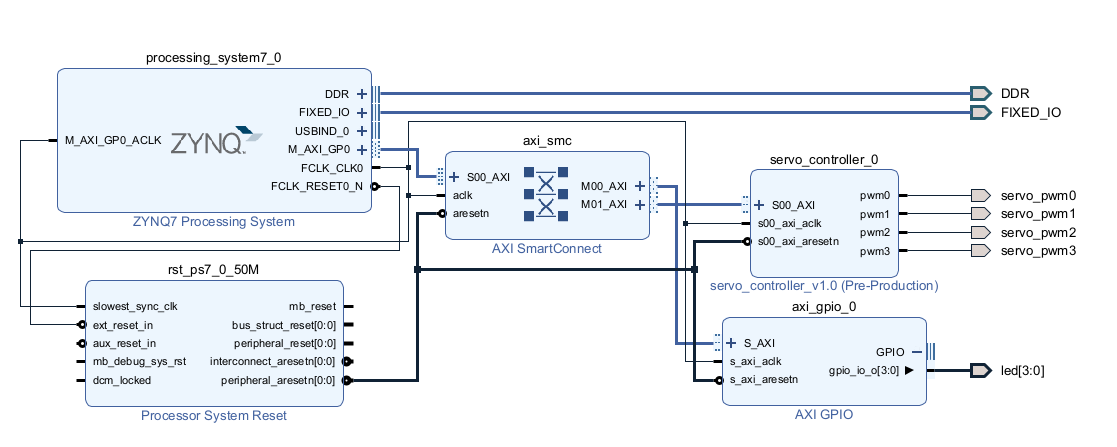
Linked from
- 6 Axis Arm Axle
- Bare metal Axle
- Petalinux Axle